

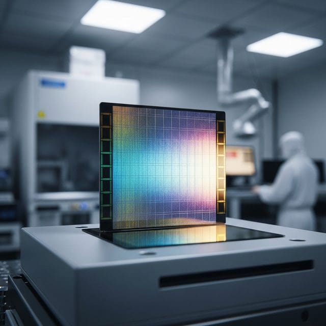
Researchers at MIT have developed a method to grow and protect atomically thin superconductors, potentially enabling the miniaturization of quantum hardware and more resilient electronic circuits.
A research team led by the Massachusetts Institute of Technology has achieved a significant milestone in condensed matter physics by successfully fabricating air-stable, ultrathin superconductors. This development addresses a long-standing hurdle in quantum computing: the extreme fragility of materials that are only one or a few atoms thick. While these materials offer unique properties for scaling down quantum hardware, they typically oxidize and lose their functionality almost instantly when exposed to the atmosphere. The new research, published in Nature, provides a path toward manufacturing these materials at a scale suitable for industrial application.
The study, led by co-lead authors Xudong Sheldon Zheng, Sameia Zaman, and Kenan Zhang, details a process where researchers grow a superconducting material called niobium diselenide underneath a protective layer of graphene. By placing the carbon-based graphene on a silicon dioxide substrate first and growing the superconductor in the nanometer-sized gap beneath it, the team effectively shielded the material from the moment of its creation. This “encapsulation epitaxy” method resulted in smooth, uniform layers of material across areas larger than an inch, a scale previously unattainable for monolayer superconductors which were usually limited to small, exfoliated flakes.
William D. Oliver, a professor of physics at MIT and director of the Center for Quantum Engineering, oversaw the project alongside colleagues Jing Kong and Joel Î-j. Wang. The team demonstrated that the resulting films maintain a high kinetic inductance—a property that allows the material to store significant energy in a very small footprint. Niobium diselenide is particularly valued for this trait, as it consists of a single layer of niobium atoms sandwiched between selenium atoms. In practical terms, this could allow engineers to replace bulky arrays of electronic junctions in quantum circuits with tiny pieces of thin-film material, leading to more compact and efficient processors.
The technical challenge of this work involved more than just growth. The researchers had to overcome the “adhesion gap” between the graphene and the substrate, which is less than one nanometer thick. By carefully tuning the growth conditions, they forced the chemical precursors to migrate into this gap, where the graphene acted as a template to ensure a perfectly smooth monolayer. Once grown, the material is naturally encapsulated, meaning it can be removed from the vacuum of the growth chamber and handled in ambient air without the immediate degradation that typically ruins such delicate atomic structures.
Furthermore, the researchers developed a specialized etching technique to ensure reliable electrical connections between the nanometer-thin superconductor and standard electrodes, which are often hundreds of nanometers thick. By etching the side walls of the film in a vacuum, they preserved the integrity of the superconducting edge. Testing revealed that the material’s superconducting properties remained intact even after being integrated into microwave circuits. The team reported a charge-density-wave transition near 177 K and a sheet kinetic inductance of approximately 0.7 nH/□, confirming the material’s viability for fluxonium qubits and microwave photon detectors.
This advancement moves ultrathin superconductors from the realm of delicate laboratory curiosities toward viable industrial components. The team confirmed that this growth strategy can be extended to other 2D materials, including those grown under hexagonal boron nitride templates. As the global race for quantum supremacy intensifies, the ability to manufacture stable, wafer-scale quantum materials provides a critical foundation for decentralized innovation and the next generation of high-performance computing. Future work will focus on integrating these films into functional architectures for ultrasensitive detectors and advanced communication systems, potentially revolutionizing how we approach national security and scientific exploration.

Mason Reed serves as a Staff Writer for Just Right News, where he spearheads the Future Frontiers & Special Projects desk. In an era defined by rapid technological shifts and evolving social landscapes, Mason provides a steady, principled voice, examining the innovations of tomorrow through the lens of traditional American values. His work is most prominently featured in his signature series, “The Next Horizon,” where he explores the intersection of emerging technology, national sovereignty, and the preservation of individual liberty.
A native of San Diego, California, Mason’s worldview was shaped by the unique culture of his hometown. Growing up in a region defined by its strong military presence and its history of maritime industry, he developed a deep-seated respect for the institutions that provide national stability and the entrepreneurial spirit that drives the American economy. This upbringing instilled in him a belief that true progress is not found in discarding the past, but in building upon a foundation of proven principles. His reporting often reflects this San Diego influence, emphasizing the importance of a robust national defense and the necessity of maintaining a competitive edge in the global marketplace.
Now based in San Francisco, Mason operates from the heart of the world’s technological engine. Living and working in the Bay Area provides him with a front-row seat to the advancements—and the ideological challenges—emanating from Silicon Valley. While many in the region embrace a “move fast and break things” mentality, Mason’s reporting serves as a vital counterweight. He offers Just Right News readers a “boots on the ground” perspective, documenting how radical local policies and the concentration of tech power impact the everyday lives of citizens. His proximity to the industry allows him to cut through the marketing jargon of big tech to uncover the real-world implications for privacy, free speech, and the nuclear family.
In his “Future Frontiers” beat, Mason tackles complex subjects ranging from the ethics of artificial intelligence to the burgeoning private space race. He approaches these topics with a healthy skepticism toward centralized bureaucracy, championing instead the decentralized innovations that empower individuals. Through “The Next Horizon,” he highlights the pioneers and thinkers who are working to ensure that the future remains a place where human dignity and constitutional rights are protected. He believes that the rapid pace of change requires more than just technical expertise; it requires a moral compass rooted in the Western tradition.
Throughout his tenure at Just Right News, Mason has remained committed to the idea that the future is something to be shaped, not merely accepted. His writing is characterized by a rigorous defense of American exceptionalism and a belief that the country’s best days lie ahead, provided it remains true to its founding ideals. Whether he is investigating the impact of automation on the American workforce or profiling the next generation of aerospace engineers, Mason Reed ensures that his readers are equipped with the insights they need to navigate a changing world with confidence and clarity.